
config of a semiconductor wafer back grinding equipment manufacturer Grasping strong production capability, advanced research strength and excellent service, Shanghai config of a semiconductor wafer back grinding equipment supplier create the value and bring values to all of customers.
 WhatsApp)
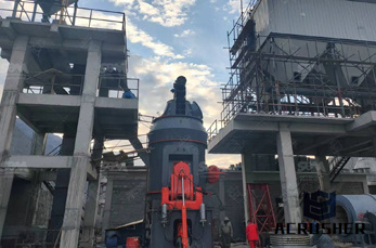
Jun 28, 2008· SEMICONDUCTOR AND MEMS PROCESS EQUIPMENT FOR CMP AND BACK GRINDING PROCESSES Axus Technology delivers semiconductor and MEMS process equipment for use with CMP processes, wafer polishing, postCMP cleaning and wafer grinding. The equipment is either new or refurbished and operates to original OEM specifications.
The TAIKO process is the name of a wafer back grinding process that uses a new grinding method developed by DISCO. This method is different to conventional back grinding. When grinding the wafer, the TAIKO process leaves an edge (approximately 2 mm) on the outer most circumference of the wafer and thin grinds only the inner circumference. By using this method, it lowers the risk of thin wafer ...
Best Equipment for advanced DicingGrinding Service. DISCO''s highquality precision technology guarantees excellent processing results. Manufactured at the Kuwabata Plant in Hiroshima Prefecture, DISCO''s precision dicing saws and grinding/polishing machines, combined with etchers, surface planers and AOI tools, offer customers the highest level of quality.
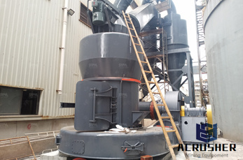
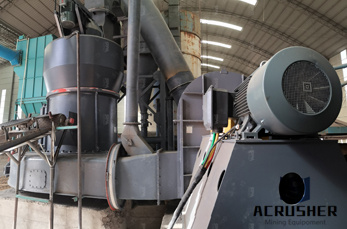
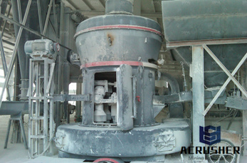
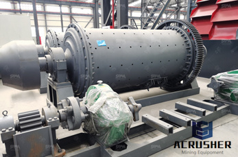
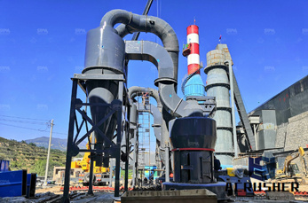
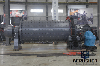
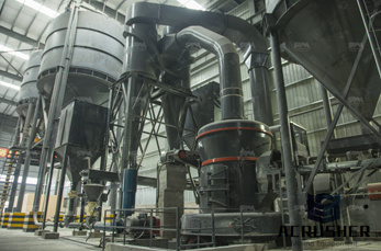
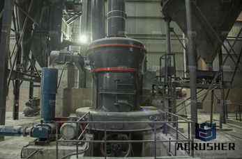
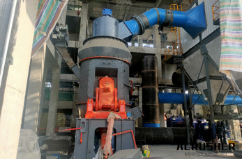
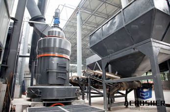
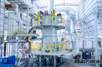
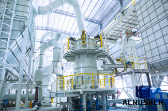
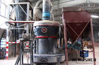
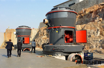
Back grinding semiconductor wafers. The best in wafer tolerances and minimum damage ... Back grinding processes Machine configuration Grinding wheels 4. config of a semiconductor wafer back grinding equipment. config of a semiconductor wafer back grinding equipment,Manufacturer of Grinding, Lapping, and CMP MachinesMachine. Tool. Semiconductor ...
Apr 28, 2017· Our "RAD3510F/12" is a system that laminates tapes for protecting the circuit sides of wafers during back grinding or thinning process of wafers after circuits are formed on them. It reduces the risk of damage during inline wafer transport and is capable of handling both wafers with bumps and ultrathin wafers.
OKAMOTO CORPORATION, Semiconductor Equipment Division provides Sales Service for Wafer Back Grinder for SiGeAlticGaAsSOISilica, Polisher, Pitch Polisher, Lapper, Slicer and SemiAuto Dicing machine for Semiconductor Electronics industries.
Laminated wafers are then loaded into wafer cassettes, which in turn are loaded into an automated backgrinding machine. This machine uses a robotic arm to pick up the wafers and position them, back side facing up, under high precision, computercontrolled grinding wheels.
This paper addresses an important aspect of silicon wafer fine grinding: machine design. For any commercially available wafer grinders, spindle angle adjustments based on the wafer shape ground is almost inevitable in order to achieve flat wafers.
Syagrus Systems is a leading service provider specializing in postfab processes for semiconductor and electronic component manufacturers worldwide. We have become a leader in semiconductor and silicon wafer back end processing by listening to our customers'' needs, working with them to create the solution and then exceeding their expectations.
Grinding of silicon wafers: A review from historical perspectives Peia,, Graham R. Fisherb, ... that machine the surfaces of silicon wafers. Other types of ... Only singleside grinders that grind one side of the wafer can be used for back grinding. Initially used ones are of Blanchard
During coarse grinding, typically 90% of the back grind is completed, significantly reducing the thickness of the wafer. Coarse grinding will cause microcracks and damage the silicon lattice. Fine grinding completes the back grind process and removes part of this damage. Incoming Wafer Requirements:
GDSI Full/Partial Wafer Grinding. A long list of engineering achievement allows customers to recover from process mistakes or wafer breakage. GDSI''s capabilities allow for yield recovery by grinding partial wafers or engineering development and die characterization by thinning at the die level.
The LINTEC Adwill series includes UV curable dicing tapes, high performance back grinding tapes, dicing die bonding tapes required for semiconductor packaging, and backside coating tapes. Adwill continues to make steady progress in the advancement of related equipment and unique systems.
Dec 04, 2015· The automation for this single wafer cleaning system uses two 6 DOF robots and custom mechanisms to transfer wafers from standard FOUPs into a vertical orientation for cleaning. The wafer .
Wafer Backgrind Wafer Backgrind is the process of grinding the backside of the wafer to the correct wafer thickness prior to assembly. It is also referred to as ''wafer thinning.'' Wafer backgrinding has not always been necessary, but the drive to make packages thinner and thinner has made it indispensable.
Semiconductor BackGrinding The silicon wafer on which the active elements are created is a thin circular disc, typically 150mm or 200mm in diameter. During diffusion and similar processes, the wafer may become bowed, but wafers for assembly are normally stress relieved and can be regarded as flat.
Wafer Back Grinding Tapes NONSILICONE, NONEVA BASED COMPRESSIBLE BACKGRINDING AND THINNING TEMPORARY BONDING ADHESIVE TAPES FOR BUMPED WAFERS AND SUBSTRATES WITH UP TO 250 MICRON BUMP HEIGHTS: The configuration of the temporary bonding adhesive tapes are engineered for high reliability for wafers and substrates with extensive .
Feb 05, 2016· A 300 mm wafer mounted on a standard film frame is spin coated using multiple chemistries under fully automatic control.
Fine grinding of silicon wafers requires high predictability and consistency, which requires the grinding wheel to possess selfdressing ability,, after initial truing, the wheel should not need any periodic dressing by external means. In other words, there should be "a perfect equilibrium
worldwide revenues generated by silicon wafers and semiconductor devices were billion [3] and 213 billion [4], respectively. As one of processes to flatten silicon wafers, simultaneous double side grinding (SDSG) has a great potential to meet the demands for high quality wafers at low cost [5]. This paper reviews the literature on SDSG.
Grinding Machines for Semiconductor Wafers Koyo Machine Industries developed several types of grinding machines, used in the semiconductor industry for silicon wafer manufacturing and IC production. Vertical and horizontal spindle systems are used in combination with special designed diamond grinding wheels, that cut just at the edge of the ...
Fig. 6, Fig. 7, Fig. 8 show three machine configurations for spindle angle adjustments. The small circle represents the wafer, and the big circle represents the grinding wheel. Point O and point O W represent the center of the wafer and the center of the grinding wheel, respectively.
This equipment applies protection tape on the wafer patterned surface for the backgrinding process. Fullauto type Semiauto type machines are lined up, and large size wafers are also available.
Leadingedge Tape × Equipment solution created with semiconductorrelated products ''Adwill.'' Products that contribute to back grinding processes such as back grinding .
WhatsApp)